
Solar thermal power plants
New record for multi-layer solar cells
With an efficiency of 34.1 per cent, researchers at the Fraunhofer Institute for Solar Energy Systems ISE have broken the current world record.
The highly efficient cell consists of thin semiconductor layers, a few micrometres thick, which are applied to a silicon solar cell. There are three layers in total. While conventional silicon cells absorb light with a wavelength between 800 and 1,200 nanometres, the wavelengths implemented by this triple-junction solar cell range between 300 and 1,200 nanometres. This is the advantage of the triple structure: the additional thin films absorb other solar radiation wavelengths. This enables the light to be utilised highly efficiently.
Looks like a conventional silicon cell
To produce the cells, the scientists are deploying the direct wafer bonding process. This originates from microelectronics. It is a multi-stage process in which the atoms in the thin-film materials form bonds with the silicon. This results in a cell that externally resembles a conventional silicon solar cell. “Compared with earlier results, the deposition conditions have been improved even further,” says Dr Frank Dimroth, Head of the III-V Photovoltaics and Concentrator Technology Department at Fraunhofer ISE, in explaining the new result. In addition, he adds, a new cell structure was introduced for the uppermost part of the cell made of gallium indium phosphide, which converts light even better into electricity. The previous world record for these cells was 33.3 per cent.
The development work is being funded by the German Federal Ministry for Economic Affairs and Energy as part of the PoTaSi project , which stands for “Demonstration of the potential of monolithic tandem solar cells made of III-V semiconductors and silicon”.
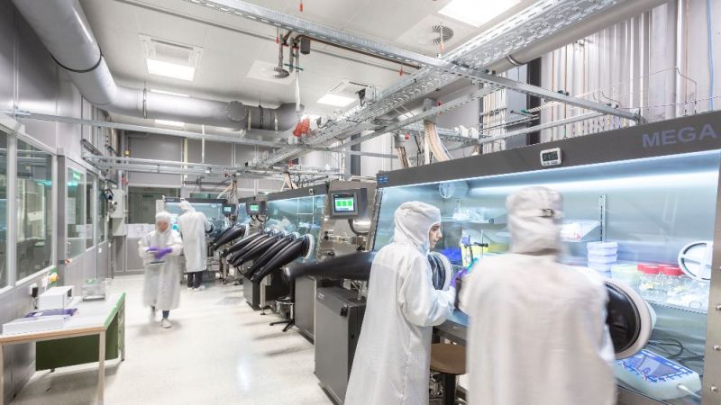


 and PERC+ solar cell (rear left) in an industrial contact burn furnace.")