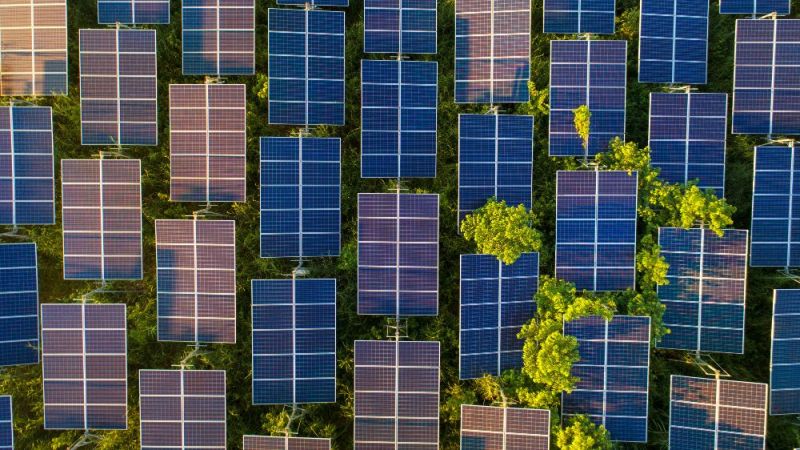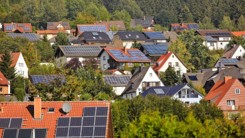
Photovoltaics
Triple solar cells achieve record efficiency
Researchers at the Fraunhofer Institute for Solar Energy Systems ISE have developed multi-layer solar cells with an efficiency of 35.9 per cent. Tandem solar cells were never so efficient. The highly efficient multi-layer solar cell consists of thin semiconductor layers, a few micrometres thick, which are in turn deposited on a silicon solar cell. There are three layers in total. This structure enables them exploit the solar spectrum more energy-efficiently than pure silicon solar cells.
High-performance silicon-based multi-junction solar cells
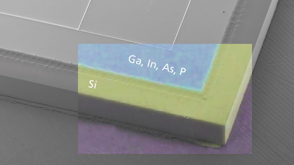
Silicon solar cells currently dominate the photovoltaic market with a share of over 92 per cent. The current efficiency of industrially manufactured silicon solar cells is between 17 and 22 per cent, with a theoretical maximum of 29.4 per cent. Higher efficiencies can reduce electricity generation costs. Less solar surface area achieves the same or even higher output. In addition, there are savings in cell and module components, such as semiconductor material, metals and frame components. This reduces both the consumption of resources and the costs. Multi-junction solar cells with silicon as the base cell and additional semiconductor layers only a few micrometres thick offer a promising approach. Silicon is a very inexpensive substrate and available everywhere. In multi-junction solar cells, the different layers absorb different spectral ranges of sunlight to make optimal use of this: Gallium indium phosphide (GaInP) between 300 - 660 nanometres (visible light), aluminium gallium arsenide (AlGaAr) between 600 - 840 nanometres (near infrared light) and silicon between 800 - 1200 nanometres (longer wave length light). This is the advantage of the solar cell that is made up of several semiconductors. The uppermost solar cell facing the light, also known as the top cell, absorbs light with short wave lengths and allows longer wave length light to pass through. The middle cell in turn absorbs part of the spectrum and lets the long-wave light through. In principle, any number of partial solar cells can be arranged on top of each other. This structure increases the efficiency of the solar cells.
Thin semiconductor layers form a unit with silicon
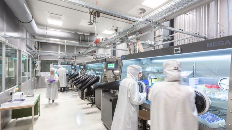
Engineers manufacture the semiconductor stacks of multi-junction solar cells using a special method called metal organic vapour phase epitaxy (MOVPE). The different materials are deposited from the gas phase onto a substrate one after the other. This process is called epitaxial layer growth. Within the PoTaSi project, short for "Demonstration of the potential of monolithic tandem solar cells made of III-V semiconductors and silicon", the researchers are epitaxially growing the top and middle cells from the semiconductor materials. They then use the direct wafer bonding method to produce the triple-junction solar cell. This is a multi-stage process, known from microelectronics, through which the atoms of the thin-film materials form chemical bonds with the silicon sub-cell. Afterwards, they are inseparably connected. From the outside, the monolithic multi-junction solar cell resembles conventional solar cells with two contacts. The stacked sub-cells and silicon are connected by tunnel diodes. The tunnel diodes serve to interconnect the subcells in series. This adds up the voltage of the cell and increases the efficiency.

Fraunhofer ISE
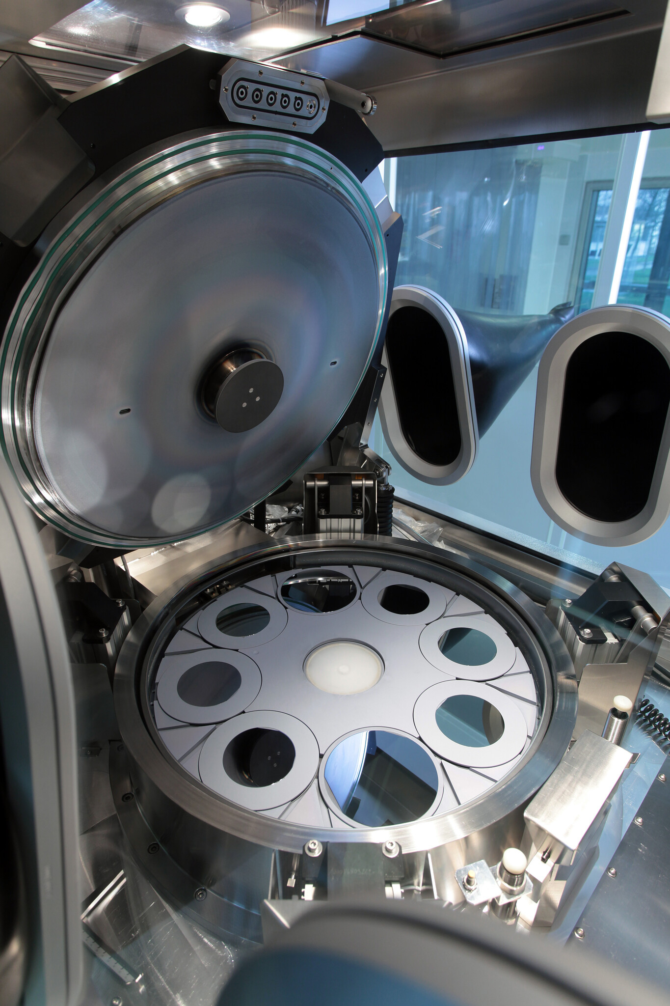
Fraunhofer ISE
Record efficiency achieved with new middle cell
In the course of the project work, the scientists were able to significantly improve almost all components of the triple-junction solar cells. First, they changed the passivation of the silicon sub-cell so that fewer charge carriers are lost. They then succeeded in optimising the GaInP top cell. In the process, it became apparent that GaInP reacts sensitively to high temperatures. The voltage of the subcell decreases and so does the efficiency. As a result, the project team changed the process flow and allowed the top cell to grow epitaxially over the middle cell. This means that the semiconductor material is exposed to lower temperatures during the gas phase epitaxy. Finally, intensive research work was carried out on the middle cell. The results contributed significantly to increasing the efficiency of the triple-junction solar cell to 35.9 per cent. The decisive factor is the use of a new compound semiconductor GaInAsP (gallium indium arsenide phosphide). This helps to substantially extend the lifetime of the load carriers. This results in the cell reaching a higher voltage.
The future of triple-junction solar cells
The project has shown the potential of the technology. First of all, the monolithic triple-junction solar cell developed is suitable for special applications where high output per area is particularly important. This applies, for example, to electrically powered aircraft and drones.
With the methods currently in use, the scientists have pursued the goal of achieving the highest levels of efficiency. The next step is to improve the manufacturing processes towards more cost-effective processes. It will therefore still take some time until the cells and modules are available on the market.
Last updated: 25.10.2021


 and PERC+ solar cell (rear left) in an industrial contact burn furnace.")