
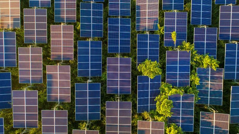
Photovoltaics
NexWafe plans gigawatt factory in Bitterfeld
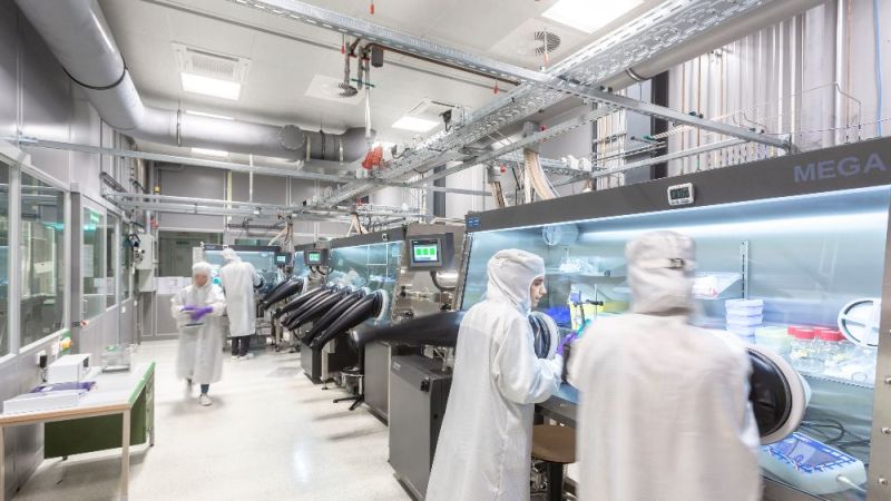
The company NexWafe wants to enter photovoltaic mass production with its alternative wafer manufacturing process in 2022.
The basis for this is years of research and development. The result is a method that clones high-quality monocrystalline silicon wafers - and at a speed that is economically mandatory for photovoltaics: The required throughput is several thousand wafers per hour. In contrast to conventional wafer production, this method produces significantly less waste and consumes less energy. The low cost and high quality of the wafers means that they can also be produced in Germany using this method: "We want to bring photovoltaics back to Europe", says managing director Dr Stefan Reber.
The basis is a method called epitaxy, which is used for instance in microelectronics. However, in order to achieve the required throughput for photovoltaics, it had to be fundamentally revised. Research questions are still pending. In December 2019, NexWafe and its partners launched the project Epi-Inspec. Here the project partners adapt the quality control measures to the new method. "The measurement technology is not 1:1 comparable to the usual production method because the manufacturing chain is different", explains Dr Kai Schillinger, project manager at NexWafe. "And right now we are at a point where we have to ensure that we deliver consistently high quality for our future customers." Project partners include for example equipment manufacturers who build the measurement technology, as well as research institutes who tailor the methods to the new wafers.
Patents and know-how as a basis for the photovoltaic start-up
Important preliminary work in the development of the wafer manufacturing process was conducted at the Fraunhofer Institute for Solar Energy Systems ISE - the NexWafe start-up is a spin-off of the research institute. "There has already been a veritable flood of patents", says managing director Dr Stefan Reber, who is also a former department head at ISE. The patents are now licensed to NexWafe. Together with the developments that were added later, there is now a patent portfolio of more than a dozen patent families, for instance relating to the epitaxy of silicon. It contains about 20 approved individual patents and others that are pending. But the secret know-how is just as important, said Reber: "There’s also secret knowledge that we protect - because although patents do protect against imitators, they are also published."
Bitterfeld has a long tradition in the chlorine-based chemical industry, one of the reasons why NexWafe will produce here. The chemical chlorosilane, which is used as a starting material, is available in large quantities at the chemical park. Furthermore, NexWafe has also acquired a polysilicon factory in Bitterfeld that is no longer in production. Its recycling plant is to be used in future to recycle a high proportion of the process gases produced. "The operating staff on site are currently preparing the plant for use with an epiwafer factory", says Reber. Construction is scheduled to start in the first half of 2021.


 and PERC+ solar cell (rear left) in an industrial contact burn furnace.")