Photovoltaics
New screen printing process for ultra-thin contact fingers for efficient silicon solar cells
The current that is generated in silicon solar cells is conducted via metallic electrodes on the front and back sides of the cells. A standard method for applying these contacts is the screen printing process. This furnishes the surface of the cell with a fine contact grid that contains large amounts of silver. The narrower the printed contacts are, the less silver is used. This reduces the cost of the silicon solar cell. Scientists developed a new screen printing process in the FINALE project, which stands for “Development of industrial printing processes for the production of ultra-fine line contacts for highly efficient silicon solar cells”. This enabled them to reduce the width of the fine contacts from 40 to 19 microns and save up to 30 per cent of silver.
Project context
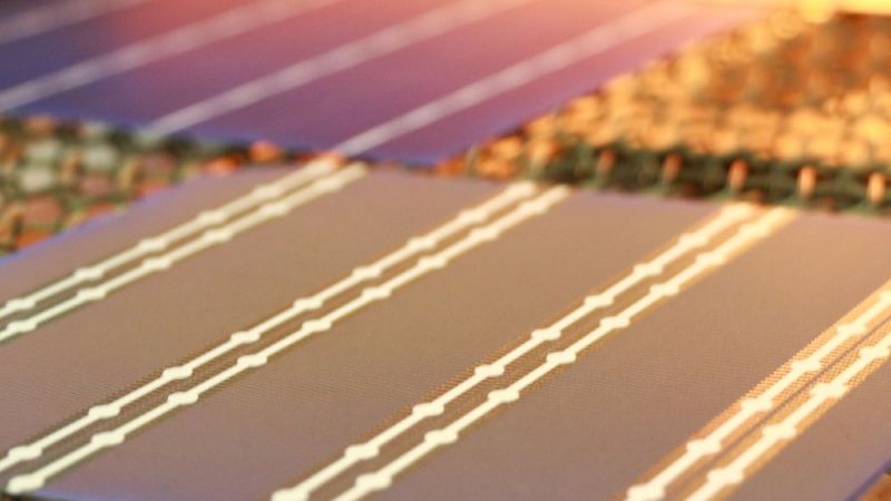
At the start of the project, the average width of the contact fingers on silicon solar cells was around 40 micrometres. A contact finger is a highly conductive and fine contact grid on the front side of a solar cell that shades as little active cell area as possible. Narrow, uninterrupted contact fingers require less material, lead to lower conduction losses and ultimately lower production costs. Highly developed special screens and metallisation pastes are required to print such fine contacts. The process is very complex and requires considerable experience. The aim of the project was therefore to optimise individual process steps and, at the same time, improve the efficiency of silicon solar cells and save costs.
Research focus
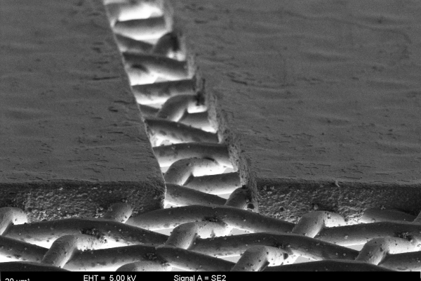
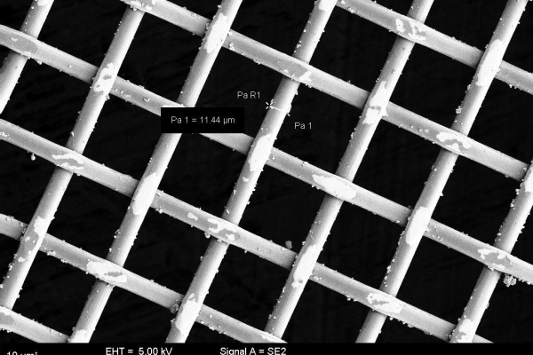
In close collaboration with the associated partner Kissel + Wolf, the project teams have succeeded in optimising the screen printing process and the screens required for printing. Their goal was to reduce the width of the contact fingers to less than 20 micrometres on textured silicon surfaces. In a first step, they developed a simulation model for the printing process, which identifies key factors influencing the process. One important factor, for example, is the interaction between the screen fabric and the metal paste with which the contacts are printed. The team then tested various screens to optimise the printing process and achieve the desired width of the contact fingers.
A further key concern was to integrate an inline process control unit, produced by the associated partner Wickon HighTech, into the screen printing process. This enables the contact geometry to be checked visually. In addition to the width of the contacts, the efficiency of solar cells also depends on the interaction between the geometry of these contacts and the surface structure of the solar cells. To this end, the project team optimised the chemical processes and chemicals used to texture the surface.
Innovation
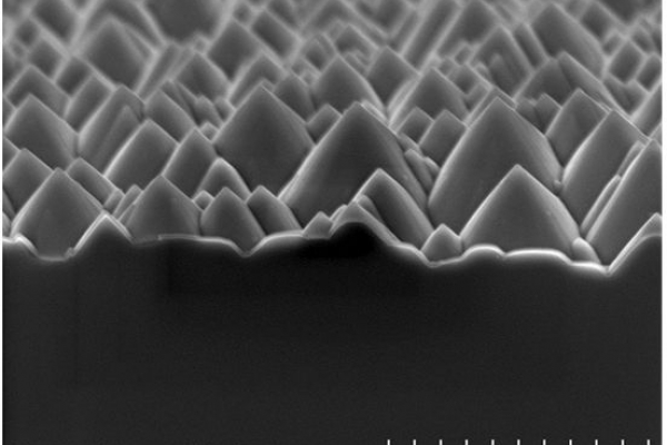
The scientists analysed the screen printing process and the existing interactions between the screen and metallisation paste, and improved the manufacturing process for the screens. As a result, it is now possible to print contact fingers with a width of less than 20 micrometres on silicon solar cells. In addition, the size of the pyramids on a textured wafer surface can be determined specifically by adding additives.
Results
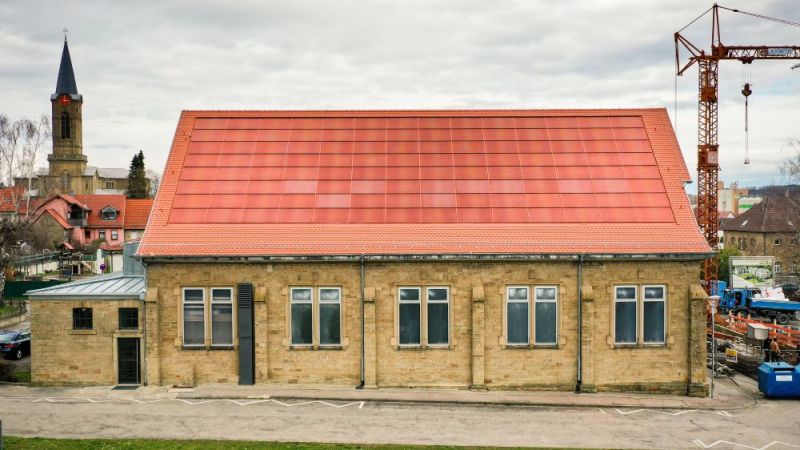
The screen printing process depends on various factors, such as the chemical composition of the materials used for the screen fabric. These influence the behaviour of the metallisation pastes. The researchers have found that optimally matched screen and paste parameters significantly improve the screen printing. This enabled the contact fingers to be printed narrower and conduct electricity better. “With the help of further developed screen and paste systems for printing the contact fingers, solar cells whose contact fingers are almost invisible could be produced industrially in the near future. This is interesting in areas where aesthetic, homogeneous module surfaces are required,” says Dr Florian Clement, department head at Fraunhofer ISE. The results from the FINALE project demonstrate the potential offered by the screen printing process, which paves the way for ultra-fine line contacts.
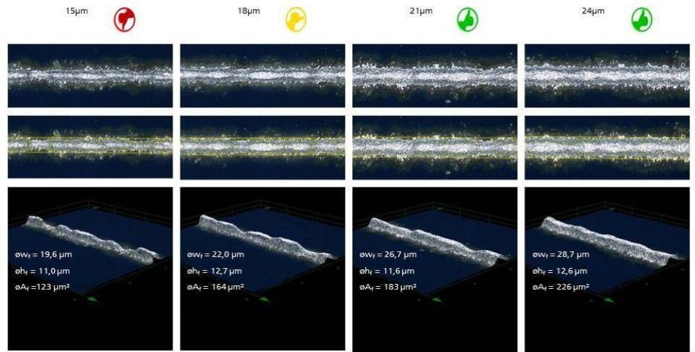
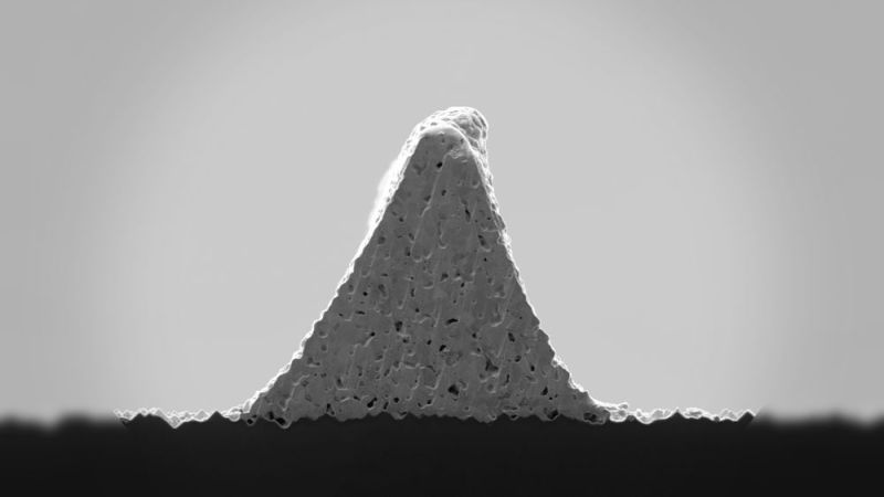
Under laboratory conditions, the researchers have already realised 16-micrometre screen openings and printed fingers with 17-micrometre widths. The geometry of these contacts is currently still too irregular. The finger resistance is therefore almost 1,000 ohms per metre. However, this value is sufficient for integrating solar cells in new module concepts that use 15 or more wires to carry the generated current instead of the 5 cell connectors conventionally used.
In a further step, the scientists printed passivated PERC solar cells on both sides. They deployed a new fine-mesh screen. This has enabled them to print contact fingers about 26 micrometres wide, which have a uniform geometry and good conductivity. The PERC solar cells have achieved a 22.1 per cent efficiency.
Practical transfer
It is partly thanks to the FINALE project that screens with texture widths in the 20-micrometre range are currently being commercially manufactured and sold for producing silicon solar cells. Companies are also using screen printing processes in the biosensor and LTCC (Low Temperature Cofired Ceramics) technology fields. These target groups are therefore also considerably interested in the knowledge gained.
Last updated: 29.11.2019

